Modifications
To use the GPIOs are some Hardware modifications needed.
In this case I used the GPIOC Port because the SDRAM Bus width is only 16bit, so I can use the MDPIN[16]-MDPIN[31]. See Pin assignment.
The RTL8186 has several registers, but only one Hardware register witch will be loaded at Power On. This Register is named ICFG. You can not read or write this Register via Software.
To use the GPIOC you must set the flag ICFG[13] to 1 else the MDPIN[16] till MDPIN[31] will be used as SDRAM bus.
The Flag ICFG[13] represents the MAPIN[20] witch is the pin 161 on 208 QFP Layout or pin E1 on 256 BGA Layout.
In my case I used an Edimax 7206APg Clone (LogiLink WL0027) so it is an 208 QFP Layout.
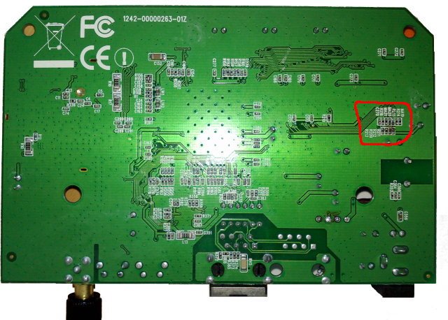
Now you have to find out where the wire goes. I don’t know if it is everywhere the same, but here it goes to the Flash Chip.
The wire goes on the backside to the middle right, marked in the picture above.
Now is the point you need a really small and good SMD solders like an Ersa Needle.
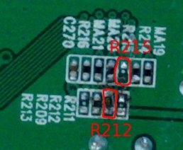
You must de soldering the resistor R215 and soldering it to R212. So you switched the ICFG[13] from low to high.
If you lost the resistor (like me) or damaged it, no problem. You can use any other 10K SMD resistor with nearly the same size. 10K SMD Resistors have a 103 printed on (10 * 103 = 10000).
Now you are finished with the register ICFG[13] and you have now 16 Digital 3,3V IO Pins.


